1. Objective:
To design simulate and analyze a BJT with a common-emitter configuration, that amplifies the voltage of an input waveform, and the emitter follower reproduces the waveform without voltage amplification, but with sufficient current to drive the low-resistance load2. Theory:
Once the transistor is biased all the operation point is know the transconductance value is known with a formula
Once g m , is calculated then AC analysis for small signal is done for the figure 1. As we can see in the figure 1 there are 2 external capacitor C2 and C1. These capacitor contribute for the low frequency poles. Also, there are internal resistance Cπ and Cμ which are responsible for high frequency poles. If we measure the frequency response of the figure 1 we can tell form the bode plot of this circuit would be a band pass filter.
3. Equipment Used
- Breadboard
- 2N2222 NPN Transistor
- DC power supply
- Wires
- Resistors and Capacitors
- LT Spice IV
4. Schematics and simulation:
There are three simulations done for the circuit. First simulation is done to find the operation point (DC simulation) of the transistor to find biasing point, second one small signal AC simulation of figure 1 and the last one is the simulation of figure 1 with capacitor C E connected at Emitter of the transistor.
The V CC for the given circuit was 5 volts whereas VEE was -5 volts. Here, the simulation shows that the collector current in the transistor is 3.47 mA. And the output voltage is -0.81 V. We know that the capacitors are open circuit for the DC calculation. Once the biasing point is known the AC simulation for small signal is done.
The figure 3 below shows the frequency response of the figure 1.
Transient response with an input of 100mv sine wave with 1 Kilohertz frequency which is shown below in figure 4 and figure 5
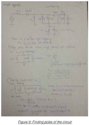
5. Hand Calculations
6. Results and Discussions
Here, the figure 10 shows the Vout measured at Oscilloscope at 200 Hz. The output voltage came out to be 38 mV. Table 1 shows the Vin, Vout recorded at the lab. After recording them we calculated the gain in Decibels and thus bode plot was drawn in figure 11. The hand calculation does not match with the simulation value. Since, the value of beta was not the same causing and error on Ic calculation. Which eventually lead to wrong calculation for the value of gm. The calculated value for gm and rπ came out to be 0.0552A/V and 2.89 Kilo Ohm .The low frequency poles calculated by hand came out to be 1.58 Hz, 16.06 Hz, 12.40 Hz where as there is huge error for the calculation of high frequency pole since, C π and C μ were not given in data sheet. Also, unity frequency wT was not successfully calculated. I assumed w T to be 100 GHz for the lab. Also, a phenomenon was observed on simulation that the gain would increase exponentially when a bypass capacitor was connected parallel to
resistance of Emitter.
7. Conclusion:
Laboratory was tricky and dealed with small AC signal. Once, the biasing point was known AC signal is added on the circuit. Then, gain was calculated for the given AC signal. Interestingly , found out that the gain would increase dramatically when a by capacitor is added to Emitter of the transistor.


Thanks man!!
ReplyDeleteThanks and I have a super proposal: House Renovation home renovations near me
ReplyDelete